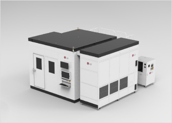
Semiconductor
- Laser Applications
- High-precision laser processing and thermal treatment
- Deposition
- Techniques to confer electrical characteristics to surfaces
- Coating
- Uniform distribution of liquid materials on substrates
- Patterning ・ Exposure
- Technologies for circuit patterning without the need for photo masks
- Precision Assembly
- High-speed, high-precision attachment during packaging and testing
- Inspection
- Real-time and post-process inspection of defects, shapes, and alignment
Ceramic Scriber & Breaking
Semiconductor / display scriber & breaking precision processing technology
- Optimized tact time with reliable logistics configuration
- Equipment configuration capable of producing multiple models
- Precise and stable breaking through 3-axis interpolation technology


Glass Laser Scriber & Breaking
Semiconductor / display glass laser scriber & breaking technology
- Multimodal auto change associated with parent systems
- Process abnormality monitoring and calibration technology
- Optimizing breaking process with 3-axis interpolation technology

UV Laser Drilling
Semiconductor / display UV laser drilling precision processing technology
- Enhancing productivity by applying AOD technology
- Minimizing defects with Cu layer detection function
- Providing high precision via manufacturing technology through optimal optical calibration system
TGV(Through Glass Via) Laser Drilling
Semiconductor / display TGV laser modification technology
- Minimizing defects by applying real-time quality monitoring technology
- Developing high-efficiency production system with AI scan path tracking technology
- Minimizing wall micro cracks through optimal optical system
Laser Trimming
Semiconductor / display laser trimming precision processing technology
- 4 head layout optimization → reduce production area and maximize productivity
- Large area high-speed processing (200x200mm)
- CTQ automatic calibration equipment (narrow bezel implementation)
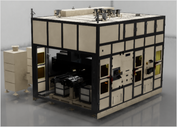
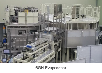
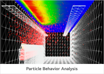
Plasma Application Vacuum Technology
System optimization technology through Simulation
(electric field, thermal, flow, particle behavior analysis)
- Development of various substrate sizes and process technologies (300mm wafer ~10.5G glass substrate)
- Substrate pretreatment technology for improved adhesion (atmospheric pressure / vacuum plasma, vacuum ultraviolet)
- Hydrophilic, hydrophobic and organic etching technologies using atmospheric pressure plasma
Use Case PECVD / ALD / sputter for solar, sputter / plasma treatment for OLED


Digital Printing Technology
Thin film or pattern printing by spraying functional ink with digital signal processing
- Minimize material consumption with maskless selective printing
- Print quality monitoring and calibration technology
- Flexible process by digital image processing
Use Case LCD PI, LCD / OLED bezel, OLED encapsulation, OC coating, metal patterning

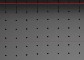
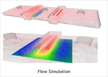
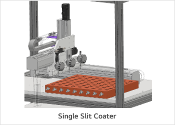
Precision Coater
Technology for coating a large area with a functional solution with a thickness of 10㎛ or less
- Semiconductor / secondary battery / medical film precision slit coater technology
- Uniformity ensured by applying multiple feed sources for precision and large-size products
- Auto-leveling function for coater and table flatness correction
- Custom design of slit coater discharge section for 3D shape coating
- Optimization of slit coater system through fluid analysis
LDI(Laser Direct Imaging) Lithography Technology
Technology that implements high resolution patterns on substrates without photo masks
- Capable of implementing high resolution pattern (line & space 1.5㎛)
- Real time pattern generation and calibration function (monitoring & calibration)
- Projection lens technology, precision alignment technology, stage technology
- Applicable to semiconductor advanced package, display (various types, multi-variable small quantity), MEMS, etc.
Use Case Display for PDP / LCD / OLED, PCB for R&D
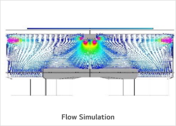
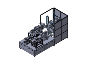
ATD(Advanced Thermal Materials Dispensing) System
Thermal management technology to upgrade and maintain product quality by applying heat interface solutions precisely and quantitatively
- Providing dispensing solution tailored to product characteristics, shape, and etc.
- Optimizing dispensing system through fluid analysis
- Developing high efficiency production system considering capacity and footprint
- Minimizing defect by applying AI inspection technology
- ATD Dispenser - Apply TIM paste using one-shot dispensing technology (AVN, telematic, SSD, etc.)
- Ag Paste Dispenser - Combining one-shot dispensing and scrapping technology to reduce paste consumption and ensure flatness (automotive semiconductors, semiconductors, etc.)
- ATD Nozzle - ANSYS FLUENT analysis tool ensures uniformity of application through optimal design
Attach
Providing technology for high speed / precise attachment of various parts of the camera / laser module
-
High-precision attach technology
- Precise attachment technology through force control
- Equipped with precision attach offset applied technology through AI technology -
Provide high speed solution
- High speed motion control
- Developed equivalence measurement unit of vision and laser displacement sensor
- Various type of application patterns though dual dispensing unit -
Adhesion degree inspection technology
- Application of high-speed adhesion inspection technology -
Customer oriented platform
- Flexible change of dispensing unit quantity according to customer needs
- Selective batch / in-line equipment configuration
- Material-tailored UV curing structure - SW with auto teaching / setting
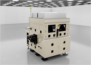
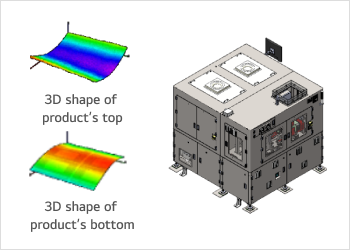
PKG Mold Thickness Measurement Equipment
Simultaneous measurement of 3D shape on top and bottom of the product and thickness calculation equipment (new excellent technology certified, patented)
- Ultra-precise moiré measurement optics and algorithms
- High-speed image processing and logistics mechanisms
- Non-contact thickness measurement and inspection for products requiring precise quality control
- Equipped with automatic calibration to ensure long-term measurement stability
Use Case Memory package mold thickness measuring equipment
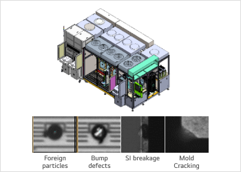
PKG Chip 6-side Inspection Equipment
Package chip (HBM, DRAM) 6-sided high-speed and high-precision inspection equipment
-
Chip appearance inspection functions
(mold damage / crack, chip dimension, bump damage pitch / offset, FM, chipping, etc.) - Silicon surface inspection functions (dimple, dent, scratch, delamination, etc.)
- Special features : bump co-planarity, surface 3D profile (dimple), Si-mold delamination
- Product unloading & loading (FOUP, tray, reel)
Use Case Memory package chip 6-side inspection T&R equipment
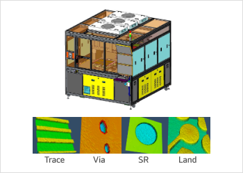
PKG Substrate 3D / 2D Composite Inspection Equipment
High-precision 3D measurement + high-speed 2D inspection
- Providing total solution from foreign matter / cracks in bare glass, TGV hole measurement, plating pattern inspection, to SR layer bump height measurement
- Capable of dealing with minimum line width of 1㎛ (high-ratio line width & height can be measured)
- High measurement repeatability + AI defect type classification
Use Case FC-BGA substrate 3D measurement / 2D inspection, glass core TGV hole inspection