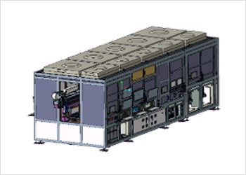
Display
- TFT
- Formation of transistor circuits for pixel control in LCD / OLED displays
- Deposition ・ Encapsulation
-
Deposition : Layering of functional materials to
form circuits or emission structuresEncapsulation : Protection of circuits and emission layers from
oxygen, moisture, and dust
- Module
- Final process of assembling display panels into deployable product units
Photo Lithography
Technology for implementing micro-patterns on an object using a UV light source
- Optical illumination technology that implements large-area parallel light
- Alignment technology for precise alignment between patterns and maintaining gap between mask and target
- High-stiffness dual stage technology for micro-pattern repeatability


Ceramic Scriber & Breaking
Semiconductor / display scriber & breaking precision processing technology
- Optimized tact time with reliable logistics configuration
- Equipment configuration capable of producing multiple models
- Precise and stable breaking through 3-axis interpolation technology

Glass Laser Scriber & Breaking
Semiconductor / display glass laser scriber & breaking technology
- Multimodal auto change associated with parent systems
- Process abnormality monitoring and calibration technology
- Optimizing breaking process with 3-axis interpolation technology
Laser Trimming
Semiconductor / display laser trimming precision processing technology
- 4 head layout optimization → reduce production area and maximize productivity
- Large area high-speed processing (200x200mm)
- CTQ automatic calibration equipment (narrow bezel implementation)
Excimer Laser Annealing System
Process for improving the electron transfer speed of OLED displays
- Quality monitoring features for improved yield
- Zero quality issue by applying Mura-Free process technology
- Diversifying process conditions by applying extreme vector scan technology
Micro Linewidth Review Laser Repair
6G mother glass panel review & repair technology
- Selective/precise processing using femto-second laser
- Capable of general use with slit & scanner optics
- Minimize operator-caused errors with macro path setting feature
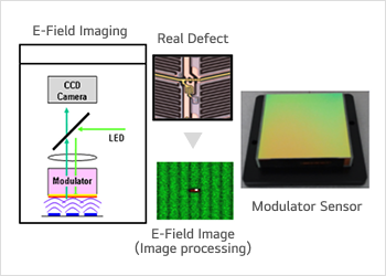
Array Tester
LCD, OLED back plane panel pixel, circuit defect inspection equipment
- Defect detection electric field sensing technology (Modulator Sensor)
- Modulator levitation technology for maintaining 30𝑢𝑚 air gap
- High-resolution optical technology of electric field-sensing images
- High-precision proving technology for signal acquisition on the panel
- Image processing and detection algorithm technology for defect detection
Use Case LCD TFT-oriented inspection equipment (mobile, TV, Auto)
OLED back plane-oriented inspection equipment (mobile, TV, Auto)
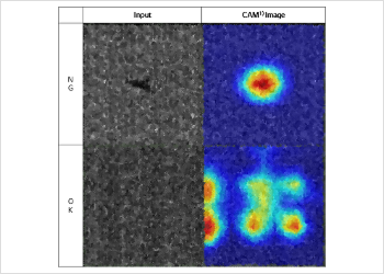
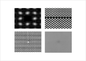
2D AOI(Automated Optical Inspection) Pattern Inspector
Display panel inspection using high-resolution 2D optical system
- MURA and pattern anomalies (open / short / etc.) and foreign object complex inspection capabilities
- High speed / flying review function
- AI-based defect classification function and YMS(Yield Management System) integration
Use Case High-resolution line camera (RGB / mix lighting), High-resolution area camera (multi-condition) optical solution
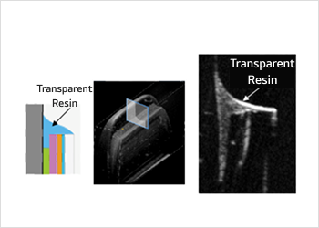
High Resolution Encap. Inkjet(Encapsulation Inkjet for pOLED) System
A core OLED process that utilizes high-resolution inkjet printing technology that applies thin film encapsulation process to coat OLED with a thin, transparent protective film
- Precision Printing with High Resolution Head Module
- Real-time monitoring with high speed drop inspection technology
- Stain correction technology for stain-free quality
- Equipped with SW technology to control specific areas and implement free shape patterns
- PRI Head Controller Design
EHD(ElectroHydro Dynamics) High-Precision Micro Printing Technology
A printing technology that transforms the liquid surface (meniscus) by applying electric force to the nozzle.
- Display / semiconductor high-precision high-definition printing technology
- Implementation of ~𝑢𝑚-level ultra-fine high-speed coating through electric field
- Optimization of spreading through fluid / flow analysis
- Nozzle auto calibration & real-time printing control
- PRI motion algorithm applied free shape printing
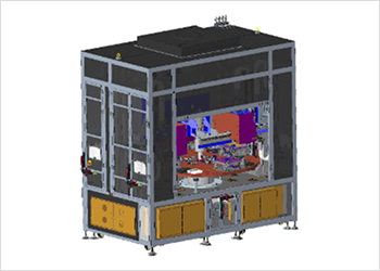
Vacuum Fusion Laser Patterning System
EL patterning technology for improving OLED display luminance deviation
- Provides laser process solutions in vacuum environments
- Supports complex processes with upper / lower dual laser irradiation method
- Optimization of foreign object control through simulation and analysis of foreign object behavior in the chamber
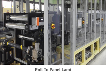
Film Laminating
Film lamination technology for mobile, IT, auto, TV products
- High-precision align and attachment technology, peeling technology
- Roll / drum / RTP(Roll to Panel) / screen
Optical Bonding
Optical bonding technology that bonds cover glass, panel, and film using optical adhesive material
- High-precision bonding equipment with quantitative / static pressure control and flatness compensation structure
- Pressure / heating control technology in normal pressure or vacuum atmosphere according to product characteristics
- Establishment of an in-line high-efficiency production system for logistics automation and continuous process
Micro LED Transfer Equipment
Large area high speed / high accuracy transfer for signage
- Parallel & alignment auto calibration precision transcription
- Preventing material thermal expansion through cooling technology
- High-efficiency production system considering capacity and footprint
Display Bonding (COG, COF Bonder, PCB Bonder, Micro LED Bonder)
High resolution high precision (2𝑢𝑚 level) bonding technology
- ACF material non-stop automatic exchange system
- Tool parallel automatic measurement / calibration system
- Real-time pressure monitoring and anomaly detection system
- Real pattern measurement inspection system
- COF material thermal expansion automatic calibration system
- Variable focusing lens system
APD(Advance Precision Dispensing) System
Process equipment that performs three-dimensional sealing in micron units using functional solutions
(grounding, light leakage prevention, waterproofing, etc.)
- Real-time material tolerance and condition measurement auto calibration.
- Precise application position and volume control with a high response controller.
- Controlling the direction of application discharge through the E-flied (EHD) effect.
- Developed a dedicated nozzle and implemented a three-dimensional application shape.
- DX, digital twin process equipment is applied.
Use Case OLED panel: smart phone, tablet, monitor, TV , Auto : camera hole grounding, panel edge strengthening, light leakage prevention, etc.
Camera module, electronic module : strengthening assembly parts, application of heat resistant resin, etc.
High-Precision / High-Speed Lighting Inspector
Inspection of defects that occur during lighting of the display cell and module processes
- Provides advanced lighting inspection and classification judgment functions according to product group
- Self-developed AI inspection technology
- Product contact lighting technology
- Provides integrated inspection solution for point, line defects, stains, and viewing angle defects
- High-speed processing technology to provide multi-pattern high-speed inspection
Use Case Medium OLED CP, assembly line lighting inspection, IT LCD tablet, notebook, Monitor assembly line lighting inspection, OLED TV cell, assembly line lighting inspection
Multi-imaging Inspection Technology / Display Appearance Inspection Machine
Display module line appearance inspection automation equipment
- Multi-condition multi-imaging high-speed scan inspection
- Glass series defect inspection specialization
- Resin process series defect inspection specialization
- Learning AI defect conditions and minimizing over inspection
Use Case Cover glass inspection equipment, display module assembly line inspection equipment, camera hole ink application inspection equipment, FPCB bonding resin inspection equipment, edge crack inspection equipment, DB(Direct Bonding) inspection equipment
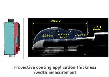
Conformal Coating Thickness Measurement Technology
Accurate thickness measurement of transparent coating layer
- Tomography using OCT technology
- Thickness measurement from floor to surface and void inspection
- Capable of real-time inspection by combining with application equipment
Use Case Flex cable protective coating thickness measurement, dustproof and moisture-proof coating thickness measurement
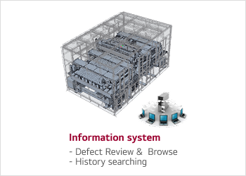
High-Resolution High-Speed Review System
6G mother glass panel defect high resolution high speed review technology
- High speed review through efficient 4 head review coordinate distribution
- Minimize review time with optimal path detection
- Improving review point efficiency through self-defect filtering